The custom PCB that handles power management and routing for each sensor node is made up of three stages: signal acquisition, conditioning and storage, and level-shifting.
Signal is acquired from the Windbelt sustainability element and sent to a half-wave rectifier, where approximately 1.8V AC at 25MPH wind gusts is converted to about 1.5V of pulsating DC.

Signal is routed into a boost converter, which is made specifically for nano-scale harvesting. It works to trickle charge a Li-Ion battery by providing 4.1V from a minimum of 550mV of AC from the power source. The boost converter also provides fail-safe mechanisms that inhibit the current produced when input voltage would otherwise drive output over the safe level of 4.2V for a lithium-ion battery.
The current is boosted when levels are lower than 3.2V through an algorithm called MPPT. This is done by continuously sampling input voltage at one of the pins of the device, and utilizing about 80% of the voltage that is sampled at the pin.
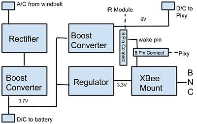
The 3.7V DC coming from the boost converter is routed to two different components: a PixyCam embedded camera and an XBee radio module. Since a different voltage is required to power each, specialized amplifiers are needed to convert 3.7V to 9V for the camera and to 3.3V for the radio.
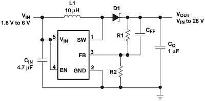
A low-power DC to DC boost converter that offers features such as low quiescent current and high gain is shown in the figure below. The boost converter is commonly used in cell phone applications, and for LCD displays to supply a high efficiency power source over the entire operating range of the attached device.
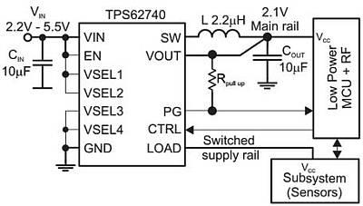
A low-noise, low-power DC to DC buck converter will be configured for a 3.3V output by using the supplied pin select configuration. The buck converter offers features such as a low quiescent current, DCS-Control, and low output ripple. Common applications include Bluetooth Low Energy, and Zigbee communication.
Attached devices operate in a variety of modes. For instance, the XBee modules are able to enter a low power state, and draw more current while transmitting data. The PixyCam has similar features, drawing more current while performing CV algorithms. For this reason, power supplies must be able to dynamically adjust the load current to meet the demands of the device, which poses a difficult design problem.
The storage element that was chosen for the project was a 15600mAh Tenergy battery pack that provides 3.7V. It is relatively lightweight, and provides overcharge and discharge protection. Coupled with a smart charger to provide initial charge conditions, it should be more than adequate. Care must be taken to provide no more than 4.2V to the battery, or risk damage and capacity decay. This risk is mitigated by providing an over-voltage threshold that is programmed into the BQ25504 boost converter.
Power Module Routing
Texas Instruments provides a BXL file that can be converted into a script that allows it to be interpreted by custom PCB design programs like EAGLE. First, transient analysis with SPICE must be performed to get an idea for all passive component values and how dynamic components should be configured for use. Then, the values used in successful simulations can be confirmed in the design of the schematic and layout in EAGLE.
There are many important factors to consider when finalizing layout, such as placement of power and ground planes. Often times they must be isolated between noise sensitive components to minimize interference.
Power Module Risks
There is still a slight risk that current from the Windbelt will be too low to work with at the boost converter level once the associated load is connected to it. Proof of concept will be provided to eliminate this concern once the primary boost converter is connected to the secondary components and tested.
Concern that the battery may be under or overvolted has also been mitigated, seeing that the battery itself has a protection circuit, and the boost converter provides protection through its configuration as well.
A new concern that is arising is the amount of noise that will be present in the circuit due to EMI and RFI. This will be mitigated by providing a multi-layer PCB design, that can help reduce overall interference by up to 20dB.
Power Module Test Plan
- Boost Converter
- Connect the boost converter via a QFN to DIP converter and test output levels when not configured for MPPT, or OV/UV with a resistive load.
- Do the same for MPPT and OV/UV.
- Add the battery and perform the same tests.
- Custom PCB
- Test for continuity.
- Test voltage levels to make sure they match the specifications for each major component.
- Li-Ion Battery
- Connect battery and test rate of discharge and cut-off functionality.
- Measure charge duration over extended periods of use.